
From Semicon West: Photoacoustic Techniques Make Waves in Integrated Metrology

Broad Trends Push Integration
How the Philips System Works
Semitool's Approach
Using Echo Pulses
Broad Trends Push Integration (Back to Top)
What is driving integrated process control forward is a confluence of several trends, company representatives at the meeting told Laboratory Network.com. They cited the emergence of copper interconnects (instead of the older aluminum), which requires that thin films of copper be deposited on near-flawless "seed" layers of copper laid down on insulating substrates. Other contributing factors mentioned were the new larger (300 mm) wafers, which require better monitoring for flatness and uniformity, and the new "low-k" dielectrics, which are more vulnerable to flaws than the older ones.
With all these new materials and processes in place "the value of a wafer is enormous once it is entirely processed," said Tom Ryan, product marketing manager for semiconductor analytical systems at Philips Analytical Inc. (Natick, MA). So preventing costly defects in the production phase with integrated metrology "is a pretty powerful drawing force," he added. Philips is one of a number of companies now introducing advanced technologies to the integrated metrology marketplace.
Philips, in fact, is a name more associated with analytical laboratory instruments—particularly its X-ray fluorescence and X-ray diffraction equipment—than with semiconductor inspection and processing. But the company has recently leveraged its core competence in X-ray analysis to introduce several X-ray tools for the semiconductor industry. And several years ago, it acquired an M.I.T. spin-off firm that had developed a proprietary photoacoustic method for measuring very thin copper films. This system "is just great" for determining the thickness of the copper seed films that are integral to the new copper interconnects, Ryan noted.
The Philips photoacoustic technology is the basis for the company's PQ Emerald instrument (so-called from the green color of the laser used by the unit), which is designed for in-line metal process control, full wafer mapping, pre and post-CMP (chemical mechanical planarization) control, and advanced metal deposition control. The unit is also a key component of a new integrated metrology machine from Semitool, Inc. (Kalispell, MT) that made its debut at the Semicon West session.
How the Philips System Works (Back to Top)
To analyze metal thin films such as copper seed layers, the PQ Emerald model bombards the films with energetic pulses from a solid state laser. These pulses momentarily heat up the films, setting up surface-acoustic waves, which Ryan likens to ripples in a pond. At the same time, a second laser light beams down on the surface and gets diffracted by the acoustic ripple pattern. This diffraction pattern, which is detected by a sensor, can be converted by the instrument to the frequency of the acoustic wave, which in turn is directly related to the thickness of the metal layer.
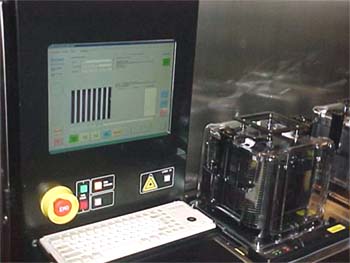
In the Philips PQ Emerald unit, shown on display at Semicon West, users insert wafers in a cassette (right) and program the machine on a computer terminal (left).
Getting a thickness reading for a single point with the Philips system takes under a second, noted Alec Reader, marketing manager for semiconductors at Philips Analytical B.V. (Almelo, The Netherlands), while mapping a whole layer on a wafer can be done in "a few minutes," he added. Older methods of gauging the thickness of metal layers on wafers, for example the "four-point" electrical probe," are not too sensitive," Reader explained, adding that they typically give mm resolution. But the photoacoustical system employed by Philips, he said, gives the same resolution as the dimensions of the ultraminiature components being measured.
The Philips measurement head is modular, so it can be used as a stand-alone inspection tool, or inserted into other instruments. The Semitool model, in which the Philips head is used, is an example of how the photoacoustic assembly can be integrated with processing functions.
Semitool's Approach (Back to Top)
Known as Paragon, the Semitool unit is a copper ECD (electrochemical deposition) system for wafer processing. It utilizes the Philips photoacoustic metrology system to measure copper seed thicknesses in order to set copper electroplating parameters in ways that result in uniform plating. Once the unit measures the seed thickness, it either sends the wafer to the ECD chamber for copper plating, the "seed enhancement" chamber for filling in holes in the seed layer, or it rejects the wafer if it is badly flawed. The Paragon system also includes an integrated chamber for back-side, bevel and edge clean, plus an integrated annealing chamber to ensure the copper layer is stabilized prior to the next step, CMP.
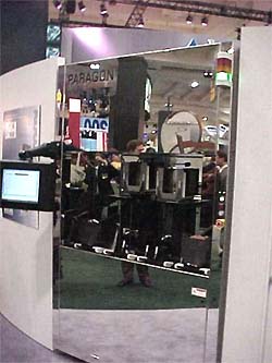
Semitool's Paragon integrated processor, shown on the floor of this week's Semicon West show, is programmed from a touch screen (left) and has anywhere from two to four cassettes, each with a capacity of 25 wafers.
Unlike older inspection methods, which required wafer fabricators to adjust their processes after the flaws had been discovered, the Semitool unit permits in-line processing adjustments. "What we do is turn wafer non-uniformity into a process parameter," summed up Tom Ritzdorf, director of ECD technology at Semitool.
While most wafer fabricators want a metal interconnect layer that is as uniform as possible, this isn't always the case, advised Dan Schmauch, product manager at Semitool. For various reasons, he noted, manufacturers may want the layer thicker or thinner on certain parts of a wafer. To accommodate these special needs, he said, the new Semitool equipment features a programmable metal deposition profile that allows users to customize the metal deposition patterns.
Overall, the Paragon system illustrates several trends in the semiconductor industry, commented Ritzdorf. One is the integration of more and more processes, such as ECD and thermal annealing, in a single unit. Another development, he added, is the emergence of more intelligent and intuitive machines. In fact the Paragon unit is "intelligent" enough, Ritzdorf said, to be able to set itself up in much the same way that the latest models of PCs are able to automatically configure new software.
Using Echo Pulses (Back to Top)
Another application of photoacoustic techniques in integrated metrology was on display at the Semicon West booth of Rudolph Technologies Inc. (Flanders, NJ). That company has had a photoacoustic metrology machine, known as MetaPULSE, on the market for several years. The unit is designed to simultaneously measure thicknesses of multilayer metal (MLM) films. At the San Francisco meeting this week, the company displayed a new "integrated" version of its existing MLM metrology unit.
While the Rudolph machine uses photoacoustics, its principle of operation is different from the Philips and Semitool devices. In fact, its underlying technology is more closely related to the sonar used by ships and submarines. Like the other methods, the Rudolph system uses a laser pulse to thermally excite a surface. This creates sound waves, which then propagate downward and bounce back. Each time a sound wave hits an interface between metal layers it is reflected as an echo. When the echo again reaches the surface it changes the surface's reflectivity. This altered reflectivity is picked up as a signal by a detector, onto which laser light reflected from the surface is beamed. The time it takes for an echo to return and be recorded as a signal is directly proportional to the thickness of the film. By successively setting the instrument to block out echoes returning after a certain preset time, users can zero in on the thickness of each layer in a multilayer structure.
According to George Collins, Rudolph's director of marketing, the new integrated MetaPULSE unit, tradenamed i-MP, is compact enough to be bolted onto a production tool such as a CMP or electroplating machine. Wafers can be inspected by the Rudolph unit before they enter the process machine or as they leave, with feedback going to the process tools in order to optimize their operation.
Typically, multilayer metal structures have been analyzed by X-ray fluorescence or X-ray reflectance. But these methods have their drawbacks, Collins asserted. The deeply penetrating X-rays make it hard to resolve one layer from another during thickness measurements, he noted. "But our system is time evolved and depth resolved," he stated. What this means, Collins explained, is that by setting the data processing component of the machine to shut out echoes returning after a certain time, users of the Rudolph technology can very precisely resolve thicknesses of all layers on a wafer. "That capability is unique," he said.
By Gordon Graff