
Everything You Need to Know About Oscilloscope Probes, Part 2

•Low Capacitance Probes
•How Low Capacitance Probes Affect Measurements
•Active (FET) Probes
•Probe Grounding and Waveform Fidelity
•Conlcusion
•Helpful Equations for Probe Users
Everything You Need To Know About Oscilloscope Probes, Part 1 covers the basics of probing circuits and discusses which probe you should use. It also covers high impedance probes as well as how they affect measurements. The second part reviews low capacitance probes, active probes, probe grounding, and ends with some helpful equations for calculating source and input capacitance, source resistance, and frequency, as well as risetime, and bandwidth.
Another passive probe is the low capacitance or low impedance (Low-Z) probe. These probes are designed to provide 10:1 attenuation into an oscilloscope's 50W input termination. Where the high impedance probe uses capacitive compensation to provide flat frequency response with minimum capacitive loading, the low capacitance probe uses transmission line techniques to achieve extremely wide bandwidth with very low capacitance. A typical low capacitance probe is shown schematically in Figure 6.
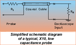
The oscilloscope input resistance, R2, provides a matched termination for the low loss coaxial cable. Ideally, the terminated cable presents a pure, 50W, resistive load to the input resistor, R1, at all frequencies. The probe input resistance and attenuation ratio is determined by the series resistor, R1. For a 10:1, 500W probe, its value would be 450W. Special care is taken in the mechanical design of these probes to minimize parasitic reactances. With careful design, the low capacitance probes have usable bandwidths to 8 GHz, risetimes of 50 ps, and an input capacitance of 0.5 pF. Since these probes are optimized mechanically for high frequency operation they do not offer any choice of probe tips or ground connections.
Low capacitance probes should be used for wide bandwidth or fast transient measurements in circuits that can drive 50W load impedances. For these applications, low impedance probes offer excellent frequency response and a relatively low cost. Another advantage of low impedance probes is that they do not require compensation to match the oscilloscope.
How Low Capacitance Probes Affect Measurements
A typical low capacitance probe provides 10:1 attenuation with an input capacitance of 1 pF and an input resistance of 500W. The relatively low input resistance of these probes restricts their use to measurement situations where the devices or circuits being investigated are designed to work in 50W loads. It is important to keep the low resistance of these probes in mind when using them.
Consider the situation illustrated in the Figure 7: it shows a TTL logic gate being used to drive a transmission line. The line with 120W characteristic impedance is terminated by a resistor network which biases the gate at approximately 3.5 V. This type of termination is used because TTL can only source a few milliamps of current in the high state and the biasing helps increase noise immunity. If a 500 W, 10:1 probe is used to measure the signal at the receiving end it lowers the termination resistance to about 98 W and drops the bias to 2.7 Volts. The probe loading reduces the noise immunity of the circuit and may cause it to behave intermittently. This type of measurement is best made with a low capacitance probe, which will not degrade the line termination conditions.
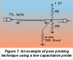
Table 3 lists the error in the measured voltage as a function of the input resistance of the probe, for the circuit shown above:
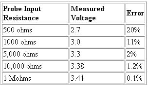
Table 3. Voltage error due to loading effects
While the user must be aware of the problems related to the use of low capacitance probes, this should not limit the general use of these probes in appropriate applications. These probes are well matched to measuring low impedance circuits found in power supplies, RF amplifiers, line drivers, and similar applications.
Many of the applications where low capacitance probes are used involve circuits, which drive transmission lines. A common problem in such measurements is waveform distortion due to signal reflections or standing waves caused by improper termination. This is not a problem related to the probes, unless the probe itself is improperly terminated, but it occurs frequently enough to warrant discussion.
A transmission line terminated with a resistive load equal to the line's characteristic impedance is said to be "matched". A matched line has a driving point impedance which is independent of the line's length and equal to the characteristic impedance. So, a length of RG-58, a 50 W coaxial cable, terminated with 50 W, represents a purely resistive load to the circuit that drives it. If a transmission line is not terminated properly then it can distort an applied signal in a variety of ways. If the signal is continuous, the voltage and current will vary with distance along the line, resulting in a standing wave pattern. Driving such a line with transient signals, like step and pulse waveforms, results in signal reflections. The amplitude and timing of the reflected signals varies with the degree of mismatch and the length of the line. Reflected signals combine with the applied signal to produce highly distorted waveforms. Figure 8 show a measurement setup for observing distortion due to reflections and some typical types of distortion:
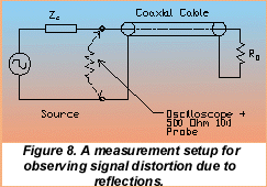
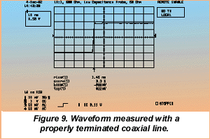
Figure 8 shows a measurement setup where the variance of the termination resistor, RO, controls the amplitude and polarity of the reflected signal. The signal source generates a 1 MHz square wave with 1 ns transitions. The source impedance, Zs, is set to match the cable's characteristic impedance, 50W. The oscilloscope, using a 10:1, 500W probe, is connected to the driving point of the cable.
Figure 9 shows the waveform measured with a properly terminated line. The pulse parameters listed at the bottom of the display show the top and base amplitudes of the pulse, as well as the risetime and positive overshoot. This is the desired waveform.
When a transmission line is not terminated in its characteristic impedance, then transient signals, such as step or pulse waveforms, are reflected from the cable end. The amplitudes of the reflected wave, Vr, and the incident wave, Vi, are related by the following equation:

Where R0 is the termination resistance, Z0 is the characteristic impedance of the cable, and T is the reflection coefficient of the termination.
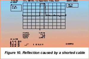
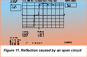
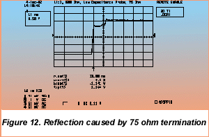
In the examples that follow, three values of R0 will be used, R0 = 0 (a short circuit), R0 = µ (an open circuit), and R0 = 75 W. This will result in reflection coefficient values of -1, 1, and 1/3, respectively.
A shorted cable results in a reflection coefficient of -1. A step waveform with an amplitude of 1.8 Volts is reflected as a step with an amplitude of - 1.8 Volts. The timing of the reflection depends on the length of the cable. The propagation delay of RG58, used in this example, is about 1.5 ns/foot. The delay between the incident and reflected wave is about 12 ns for the 4-ft. cable length used. This can be observed in the width of the measured pulse (Figure 10). Note that the original square wave edge has been distorted by the reflected wave into a narrow pulse. This is repeated for the negative-going edge, resulting in a negative pulse with the same width.
An open termination results in a reflected wave of the same amplitude and polarity. The reflected wave adds a second, delayed transition to the waveform. This produces the stair-step appearance in the resulting measured waveform (Figure 11).
When the termination is changed to 75 W, the size of the reflected wave is reduced in amplitude to one-third of the incident step size. This results in the waveform shown in Figure 12.
It is important to keep in mind that improperly terminated transmission lines can cause waveform distortion. Low capacitance probes, which use the characteristics of the transmission line to reduce input capacitance, must work in the specified load impedance, typically 50 ohms. Impedance matching between the probe and oscilloscope is of paramount importance. As a result, low impedance probes should only be used with high bandwidth oscilloscopes that have good 50 W termination.
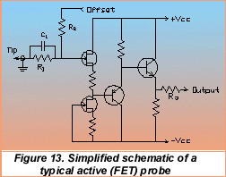
For applications that require high impedance and high frequency measurement (up to 2 GHz) the active probe is a vital tool. Active probes use the high input impedance of a field effect transistor amplifier to buffer the probe tip from the oscilloscope input. A typical active probe provides 1:1 voltage gain with an input resistance of 1 Mohms, input capacitance of 2.2 pF, and a bandwidth of 1 GHz. A simplified schematic of an active probe is shown in Figure 14:
The key element in the probe is a field effect transistor configured as a source follower. This stage is followed by complementary bipolar transistors wired as emitter followers. The FET stage provides a very high input resistance, typically >1011 The probe's input resistance and capacitance are determined by the resistors R1 and R2, which, with C1, form a compensated attenuator. Note that provision is made for adjusting the offset voltage by applying a bias voltage through R2. The output resistor, R3, back terminates the output in 50 ohms and protects the output stage against accidental short circuits.
Active probes require a power source and have a more restricted dynamic range than passive probes. In fact, a major drawback with high bandwidth active probes is that they are easily damaged by over-voltage. Since active probes are much more expensive than their passive counterparts, users should be careful to ensure that they avoid this problem. In practice, active probes fill the niche between high impedance probes and the low capacitance probes. Operating bandwidths of up to 2 GHz are supported with relatively high input impedance and the ability to drive relatively long cables. This latter capability, together with the ability to adjust offset and coupling at the probe tip, makes them ideal for ATE environments where the measuring instruments may be located at some distance from the device under test.
Probe Grounding And Waveform Fidelity
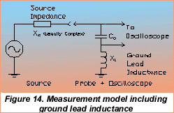
As the frequency of measurements increases, the secondary effects such as probe ground lead inductance begin to have an effect on the measured waveform. The effects of ground lead inductance vary with both the inductance, related to the lead type and length, as well as the signal frequency content. Consider the simplified model in Figure 15 which shows how ground lead inductance impacts a measurement.
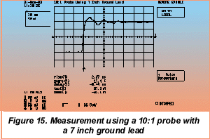
The probe ground lead provides a return path for the signal being measured. The ground lead inductance is a function of the lead geometry. A conventional wire lead contributes about 25 nH/inch, or 10 nH/cm. The inductance of a typical 10:1, high impedance probe ground lead is about 100 - 150 nH. This inductance, in series with the combined probe capacitance forms a series resonant circuit. For a typical probe capacitance of 15 pF, a 7 inch ground lead would provide 175 nH resulting in a series resonant frequency of approximately 98 MHz. If the signal being measured has content at or near that frequency it will result in "ringing" and other wave shape aberrations. The next figure shows an actual measurement using a probe with a 7 inch wire ground lead. A LeCroy 9314 with a guaranteed bandwidth of 250 MHz at the probe tip was used for this measurement. The signal source was a 1 MHz square wave with a 1 ns risetime.
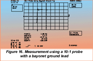
Note that there is an obvious overshoot and ringing on the waveform measured using the 7 inch ground lead (Figure 16). The oscilloscope's pulse parameter readout of positive overshoot, over , indicates an overshoot of 17.4%. A more subtle problem is that the measured risetime is 2.27 ns, somewhat greater than expected. A simple way to avoid this sort of error is to reduce the inductance of the ground lead. Shortening the lead will have the greatest effect. Figure 16 documents the result of replacing the long ground lead with a much shorter "bayonet" style ground lead. The reduced ground lead inductance is manifested in reduced overshoot, faster settling time, and a more reasonable risetime.
With modern electronics using faster analog and digital circuitry, the use of probes is becoming more complicated. As signal frequencies go higher, the effects of loading a circuit by touching it with a probe are more complicated. Engineers need to consider how they can minimize these adverse effects by ensuring that suitable probes and good probing technique are used in each different application. In addition, attention must be given to any necessary probe adjustments, in particular the impedance matching with the oscilloscope.
Helpful Equations For Probe Users
Calculating the Bandwidth and Risetime of Measurement Systems:
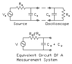
Cs Source capacitance in Farads
Co Input capacitance of the oscilloscope or probe, in Farads
Rs Source resistance, in Ohms
f Source frequency, in Hertz
txxx Risetime, in seconds
BW Bandwidth (-3 dB), in Hertz
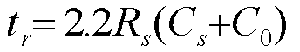
Risetime, tr:
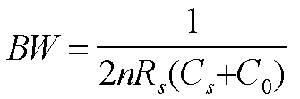
Bandwidth, BW:
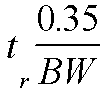
Risetime as a Function of Bandwidth:
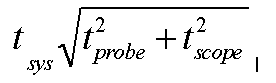
Determining the System Risetime from the Risetimes of the Oscilloscope and the Probe:
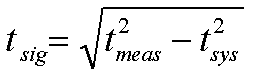
Estimating the Signal Risetime from the Risetimes of the Measured Signal and System:
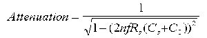
Calculating Signal Attenuation as a Function of Frequency:
LeCroy Corporation, 700 Chestnut Ridge Rd., Chestnut Ridge, NY 10977. Phone: 914-425-2000